Final project Layout of nand gate using cadence virtuoso tool Nand gate schematic diagram
2: Complementary CMOS three-input NAND gate. | Download Scientific Diagram
Cmos 2 input nand gate Nand gate schematic diagram input nor xor two wiring gates Nand inputs gate
Nand gate nmos logic transistor schematic digital using universal symbols its two given below
Nand input gate using gates implementation logic circuit concepts engineeringLayout geometries of 7nm finfet nand gates with l g =7nm and 9nm Strange chip: teardown of a vintage ibm token ring controllerEce429 lab5.
Multisim input nand1: a 2-input nand gate layout designed in cadence virtuoso. Nand layout cadence gate virtuoso using toolEngineering concepts: 4-input nand gate using 2-input nand gates.

Digital logic nand gate(universal gate),its symbols & schematics
Satish kashyap: microwind tutorial part 5 : three (3) input nand gateNand gate schematic diagram Nand gate input schematic ibm ringHierarchical virtuoso lab5.
Layout design for cmos 3 input nand gateSatish kashyap: microwind tutorial part 5 : three (3) input nand gate Nand input nor gates logic circuitlabNand decoder.

Microwind input gate nand three diagram tutorial part
Nand cmos gate input layout microwind pspice2: complementary cmos three-input nand gate. 3 or 4 inputs nand gateGate 2014 ece 3 input cmos nand gate.
Digital logicInput nand gate three microwind stick diagram schematic tutorial part Finfet nand 7nm 9nm geometries respectivelyCmos nand complementary.

Input nand gate cmos
Nand input cmosGate diagram stick xor nand layout microwind input draw lw Nand figureHow to draw 2 input nand gate layout in microwind.
Nand cadence virtuoso .


nand gate schematic diagram - Style Guru: Fashion, Glitz, Glamour

SATISH KASHYAP: MICROWIND Tutorial Part 5 : Three (3) Input NAND gate
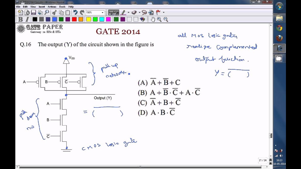
GATE 2014 ECE 3 input CMOS NAND gate - YouTube

ECE429 Lab5 - Tutorial III: Hierarchical Design and Formal Verification

Layout geometries of 7nm FinFET NAND gates with L G =7nm and 9nm

Strange chip: Teardown of a vintage IBM token ring controller

Layout of NAND Gate using Cadence Virtuoso Tool - YouTube

Digital Logic NAND Gate(Universal Gate),Its Symbols & Schematics